TeleDongle History
v0.1
The very first TeleDongle boards were built from partially-populated TeleMetrum v0.1 boards and were, not surprisingly, called TeleDongle v0.1.
v0.2
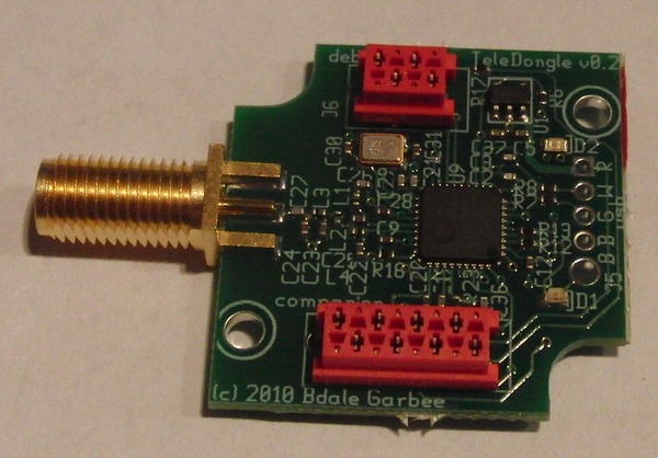
The first dedicated PCB design, made to fit in small Hammond translucent blue box, "just worked". So we put it into production and sold several hundred over time. In hindsight, we should have renamed it to v1.0 when we put it into production. Then, since v0.2 and v2.0 just seemed to confusing, when we came up with an improved version we jumped straight from v0.2 to v3.0!
Here's a photo of what the v0.2 circuit board looked like:
User View
- 70cm ham-band transceiver for interaction with TeleMetrum
- programmed for 38k4 GFSK data rate with forward error correction
- USB interface for power, configuration, and data interface
- 4 pin Tyco MicroMaTch connector for debug and flash programming
- 8 pin Tyco MicroMaTch connector supports serial or SPI interface
- 1.1 x 1.1 inch 2-layer board, fits inexpensive Hammond 1551 plastic enclosure
Developer View
- TI CC1111F32 Low Power RF System-on-Chip
- Sub-1Ghz transceiver
- 8051 MCU
- 32k Flash
- 4k RAM
- USB 2.0
- 6 12-bit analog inputs (11 bits with single-ended sensors)
- 2 channels of serial I/O
- digital I/O
- 100mA 3.3V LDO regulator
- takes input from USB interface by default
- output appears on 8-pin companion connector
- can take input from 8-pin companion connector in non-USB applications
- Software Features
- Written mostly in C with some 8051 assembler
- Runs from on-chip flash, uses on-chip RAM
- USB serial emulation for data interface
- Tools Used
- Licenses
- The hardware is licensed under the TAPR Open Hardware License
- The software is licensed GPL version 2
Artifacts
The v0.2 hardware design current gEDA files are available from git.gag.com in the project hw/teledongle.
For those who don't have ready access to the gEDA suite, here are pdf snapshots of files in more easily readable form.